选择处理器1
选择处理器2
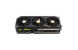
NVIDIA H100 SXM5
NVIDIA H100 PCIe

NVIDIA H100 SXM5 对 NVIDIA H100 PCIe. 规格

User rating
star star star star star
已发布
Q2/2022
NVIDIA H100 SXM5
NVIDIA H100 SXM5
已发布
Q2/2022
User rating
star star star star star
NVIDIA H100 PCIe
NVIDIA H100 PCIe

什么是最好的选择 NVIDIA H100 SXM5 或 NVIDIA H100 PCIe? 哪种显卡速度更快?

Compare the available specifications of these models.

NVIDIA H100 SXM5 has a base frequency of 1.065 GHz. 内存大小 80 GB. 存储器类型 HBM3. 发布于 Q2/2022.

NVIDIA H100 PCIe has a base frequency of 1.065 GHz. 内存大小 80 GB. 存储器类型 HBM2e. 发布于 Q2/2022.

差异

规格

技术数据
NVIDIA H100 SXM5 NVIDIA H100 SXM5
NVIDIA H100 PCIe NVIDIA H100 PCIe
一般信息

显卡的基本技术数据比较 NVIDIA H100 SXM5 和 NVIDIA H100 PCIe, 芯片,信息处理单元.

  • 建筑学
    Hopper left arrow Hopper
  • Execution Units
    8448 left arrow 7296
  • GPU芯片
    GH100 left arrow GH100
  • L1 Cache
    192 KB left arrow -
  • L2 Cache
    50 MB left arrow -
  • 渲染输出单位
    24 left arrow 24
  • 纹理单位
    528 left arrow 456
内存设置

Video memory capacity, type, bus width and bandwidth describe different properties. These values alone do not determine graphics performance.

  • Memory Bandwidth
    1,920 GB/s left arrow 1,280 GB/s
  • Memory Bus
    5120 bit left arrow 5120 bit
  • Memory Clock
    1500 MHz left arrow 1000 MHz
  • Memory Data Rate
    3 Gbps left arrow 2 Gbps
  • 内存大小
    80 GB left arrow 80 GB
  • 存储器类型
    HBM3 left arrow HBM2e
时钟频率

Published GPU clock frequencies describe different operating modes. Clock speed alone does not determine graphics performance.

  • 基准频率
    1065 MHz left arrow 1065 MHz
  • 最大频率
    1780 MHz left arrow 1650 MHz
能源消耗

Graphics card power limits and recommended system power supply describe different specifications.

  • Board Number
    PG520 left arrow -
  • System Power Supply
    1100 W (PSU recommendation) left arrow 750 W (PSU recommendation)
  • TDP
    700 W left arrow 350 W
接口

连通性和连接.

  • 最大。显示
    1 left arrow 1
  • PCIe Interface
    PCIe 5.0 x16 left arrow PCIe 5.0 x16
  • Power Connectors
    8-pin EPS left arrow 8-pin EPS
技术数据

在电脑游戏中被充分使用的技术数据.

  • CUDA
    9.0 left arrow 9.0
  • DirectX
    没有 left arrow 没有
  • 最大分辨率
    3840x2160@60Hz left arrow -
  • OpenCL
    3.0 left arrow 3.0
  • OpenGL
    没有 left arrow 没有
  • Shader Model
    没有 left arrow 没有
  • Vulkan
    没有 left arrow 没有
更多信息

GPU的接口和发布日期的比较 NVIDIA H100 PCIe 和 NVIDIA H100 SXM5.

  • Process Technology
    4 nm left arrow 4 nm
  • 发布日期
    Q2/2022 left arrow Q2/2022
Theoretical Performance

  • FP16 (theoretical)
    120.3 TFLOPS left arrow 96.31 TFLOPS
  • FP32 (theoretical)
    30.07 TFLOPS left arrow 24.08 TFLOPS
  • FP64 (theoretical)
    15.04 TFLOPS left arrow 12.04 TFLOPS
  • Pixel Rate
    42.72 GPixel/s left arrow 39.60 GPixel/s
  • Texture Rate
    939.8 GTexel/s left arrow 752.4 GTexel/s

基准

性能测试 GPUs

No comparable benchmark results are available yet. Specifications alone do not determine which model is faster.

最新比较