选择处理器1
选择处理器2
NVIDIA H100 PCIe
选择视频卡2
User rating
star star star star star
已发布
Q2/2022
NVIDIA H100 PCIe

图形卡 NVIDIA H100 PCIe, 规格

Specifications for NVIDIA H100 PCIe. Benchmark results are not available yet.

规格

技术数据
GPU
  • 建筑学
    Hopper
  • Execution Units
    7296
  • GPU芯片
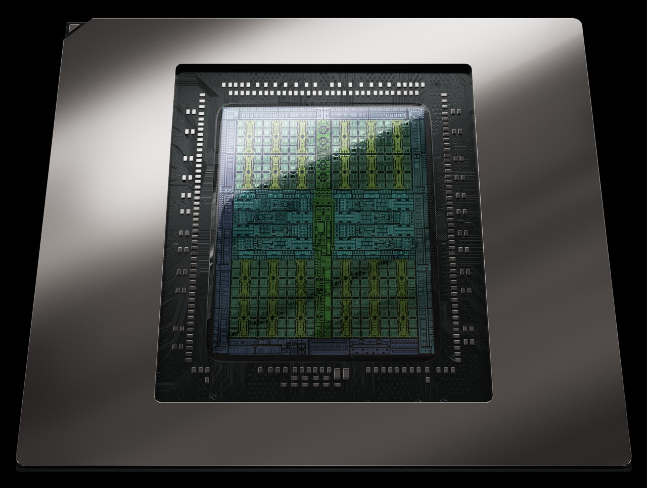
    GH100
  • 渲染输出单位
    24
  • 纹理单位
    456
记忆
  • Memory Bandwidth
    1,280 GB/s
  • Memory Bus
    5120 bit
  • Memory Clock
    1000 MHz
  • Memory Data Rate
    2 Gbps
  • 内存大小
    80 GB
  • 存储器类型
    HBM2e
时钟频率
  • 基准频率
    1065 MHz
  • 最大频率
    1650 MHz
能源消耗
  • System Power Supply
    750 W (PSU recommendation)
  • TDP
    350 W
连接性
  • 最大。显示
    1
  • PCIe Interface
    PCIe 5.0 x16
  • Power Connectors
    8-pin EPS
功能性
  • CUDA
    9.0
  • DirectX
    没有
  • OpenCL
    3.0
  • OpenGL
    没有
  • Shader Model
    没有
  • Vulkan
    没有
补充数据
  • Process Technology
    4 nm
  • 发布日期
    Q2/2022
Theoretical Performance
  • FP16 (theoretical)
    96.31 TFLOPS
  • FP32 (theoretical)
    24.08 TFLOPS
  • FP64 (theoretical)
    12.04 TFLOPS
  • Pixel Rate
    39.60 GPixel/s
  • Texture Rate
    752.4 GTexel/s
所有排名中的位置

共同立场 NVIDIA H100 PCIe 在流行的基准测试中的GPU,用于与其他模型进行比较.

No data

基准

性能测试 GPU

No benchmark results are available yet. This model is listed with specifications only.

These are saved results from the earlier catalog. Measurement dates and test configurations were not recorded. Models with no comparable results are omitted.

Recent models: test results with identified primary sources — Game frame rates

Comparable benchmark results are required to suggest performance alternatives.

*

Base Clock is the base GPU frequency stated by the manufacturer for this model.

Boost Clock describes automatic frequency increases. Actual clock speed varies with workload, temperature and power limits; it is not a guarantee of manual overclocking.

给显卡打分
NVIDIA H100 PCIe

最新比较