ロセッサー1を選択
ロセッサー2を選択
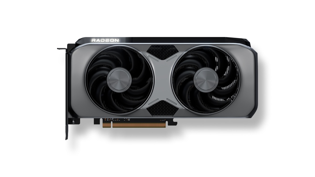
AMD Radeon RX 7900 GRE
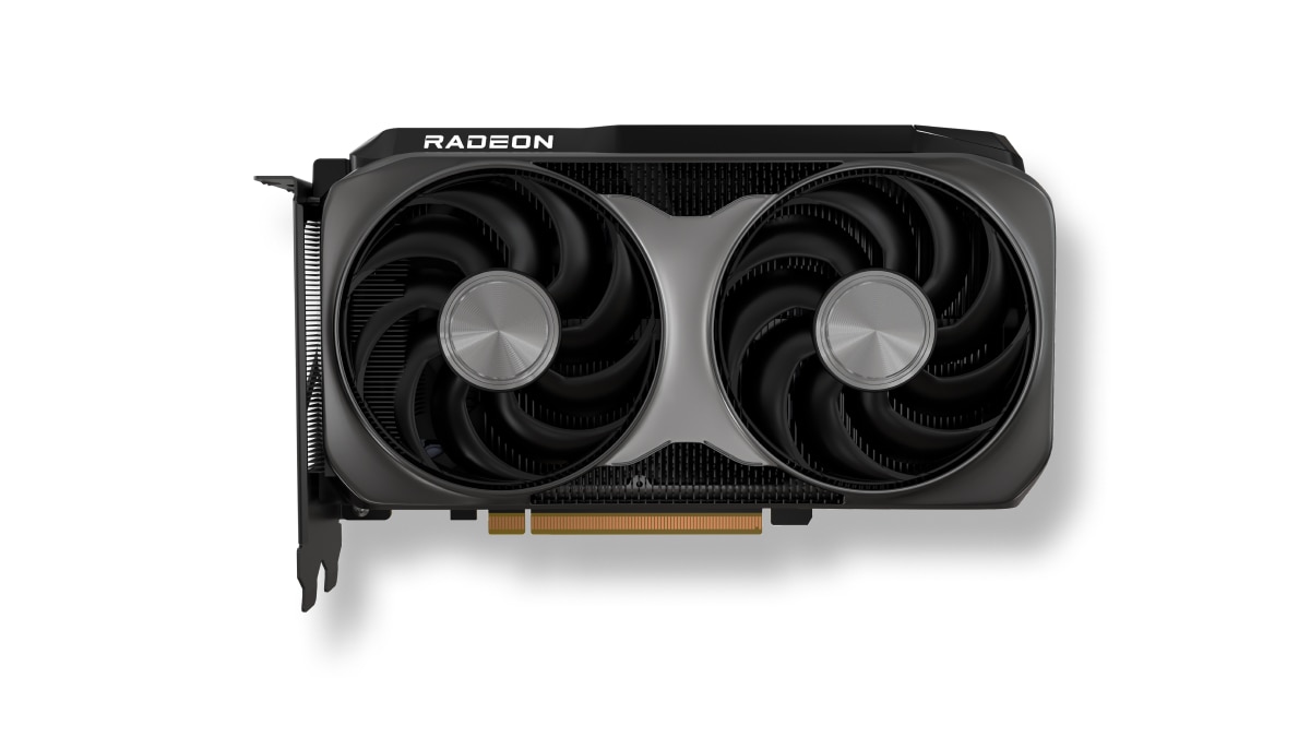
Matrox LUMA A380

AMD Radeon RX 7900 GRE 対 Matrox LUMA A380. 仕様

User rating
star star star star star
発売済み
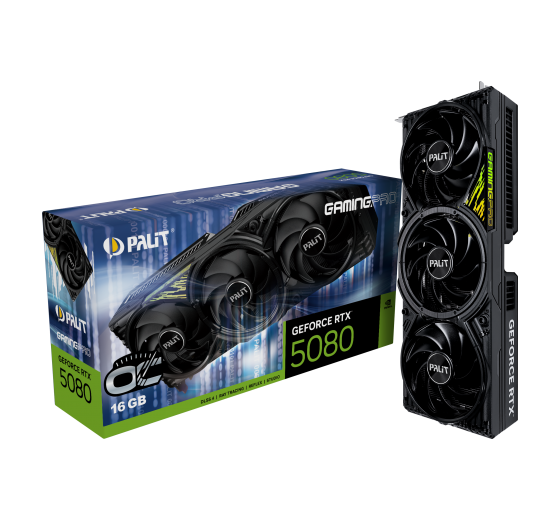
AMD Radeon RX 7900 GRE

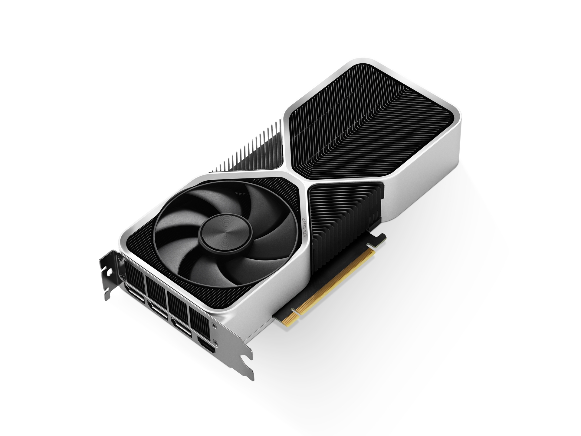
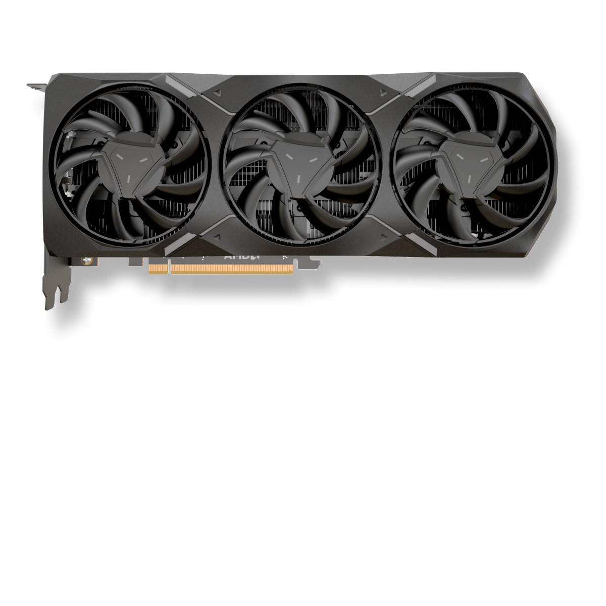
Manufacturer product image. Image source

AMD Radeon RX 7900 GRE
発売済み
Q2/2023
User rating
star star star star star
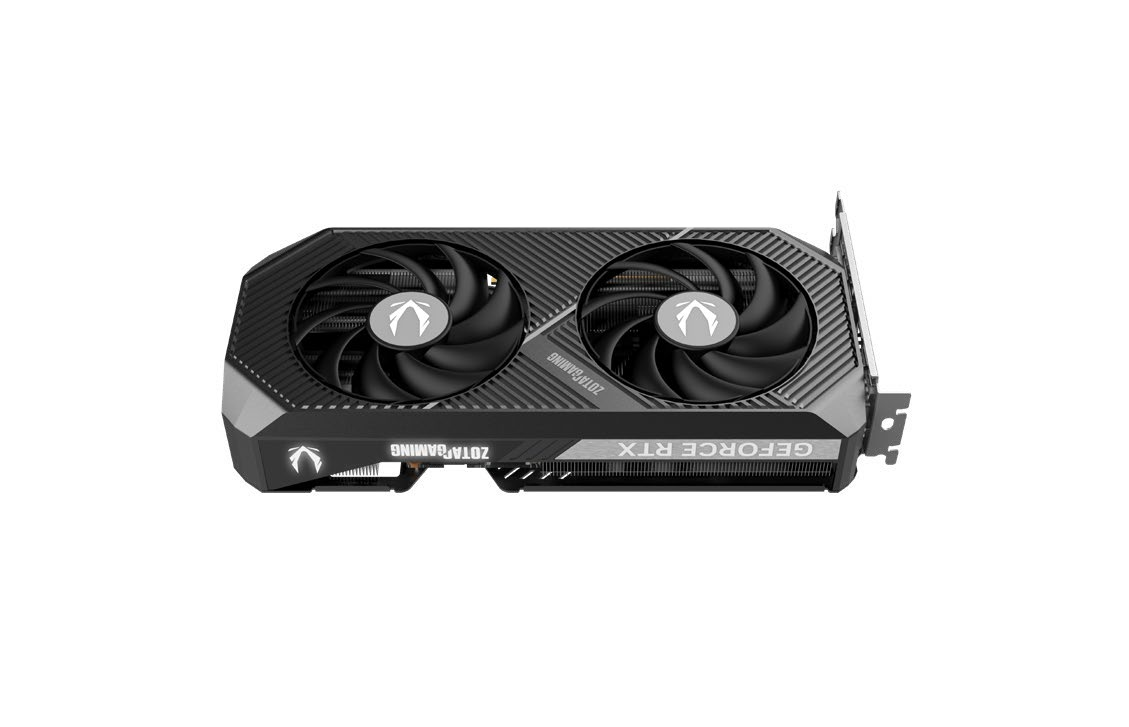
Matrox LUMA A380
Matrox LUMA A380

ベストな選択とは AMD Radeon RX 7900 GRE または Matrox LUMA A380? どのグラフィックカードが速い?

Compare the available specifications of these models.

AMD Radeon RX 7900 GREメモリサイズ 16 GB. メモリータイプ GDDR6.

Matrox LUMA A380 has a base frequency of 2.000 GHz-11 %. メモリサイズ 6 GB. メモリータイプ GDDR6. で発売されました。 Q2/2023.

相違点

  • その他のメモリ

    167メモリ増量

    16 GB left arrow 6 GB

全ランキングでの順位

共通ポジション AMD Radeon RX 7900 GRE 他機種との比較のため、一般的なベンチマークでGPUを使用。.

No data

全ランキングでの順位

共通ポジション Matrox LUMA A380 他機種との比較のため、一般的なベンチマークでGPUを使用。.

  • FP32 Performance (Single-precision TFLOPS)
    2846 place
  • Shadow of the Tomb Raider
    2857 place

仕様

技術データ
AMD Radeon RX 7900 GRE AMD Radeon RX 7900 GRE
Matrox LUMA A380 Matrox LUMA A380
一般情報

グラフィックスカードの基本技術データの比較 AMD Radeon RX 7900 GRE と Matrox LUMA A380, チップ、情報処理装置.

  • AI Accelerators
    160 left arrow -
  • Ray Accelerators
    80 left arrow -
  • シェーダー
    5120 left arrow 1024
  • Compute Units
    80 left arrow -
  • 実行部隊
    80 left arrow -
  • 建築
    RDNA 3 left arrow -
  • に基づいています。
    AMD Radeon RX 7900 GRE left arrow Intel Arc A380 Graphics
  • Raytracing Cores
    - left arrow 8
  • テクスチャユニット
    - left arrow 64
  • レンダリング出力単位
    - left arrow 32
  • Streaming Multiprocessors
    - left arrow 128
  • GPUチップ
    - left arrow ACM-G11 (Alchemist)
メモリ設定

Video memory capacity, type, bus width and bandwidth describe different properties. These values alone do not determine graphics performance.

  • Infinity Cache
    64 MB left arrow -
  • メモリ速度
    18 Gbps left arrow 15.5 Gbps
  • Memory Bandwidth
    576 GB/s left arrow -
  • Memory Bus
    256 bit left arrow -
  • メモリータイプ
    GDDR6 left arrow GDDR6
  • メモリサイズ
    16 GB left arrow 6 GB
  • メモリーインターフェース
    - left arrow 96 bit
  • Memory bandwidth
    - left arrow 186 GB/s
  • Memory Clock
    - left arrow 1.938 GHz
クロック周波数

Published GPU clock frequencies describe different operating modes. Clock speed alone does not determine graphics performance.

  • 最大周波数
    2245 MHz left arrow 2.050 GHz
  • Game Clock
    1880 MHz left arrow -
  • オーバークロッキング
    - left arrow はい
  • 基本周波数
    - left arrow 2.000 GHz-11 %
エネルギー消費量

コネクター、通常時およびオーバークロック時の放熱ワット数.

  • Power Connectors
    2x8-Pin left arrow -
  • TDP
    260 W left arrow 75 W (Reference)
  • PCIe-Power
    - left arrow 1 x 8-Pin
クーラー&ファンタイプ

グラフィックスカード冷却システム用クーラーの種類とサイズ AMD Radeon RX 7900 GRE と Matrox LUMA A380.

  • Noise (Load)
    - left arrow 0 dB
  • Noise (Idle)
    - left arrow 0 dB / Silent
  • クーラータイプ
    - left arrow Air cooling
  • ファン1
    - left arrow 1 x 70 mm
  • ファンタイプ
    - left arrow Radial
インターフェイス

コネクティビティと接続.

  • DP Ports
    - left arrow 4x DP v2.1
  • Max. 表示数
    - left arrow 4
技術データ

コンピュータゲームに活かされる技術データ.

  • Peak FP32 (theoretical)
    46 TFLOPS left arrow -
  • LED
    - left arrow No LED lighting
  • DLSS / FSR
    - left arrow はい
  • レイトレーシング
    - left arrow はい
  • DirectX
    - left arrow 12_2 (Ultimate)
  • 最大解像度
    - left arrow 7680x4320
対応するビデオコーデック

動画・画像圧縮規格に対応した内蔵型.

  • AV1
    Decode / Encode left arrow Decode / Encode
  • VP9
    - left arrow Decode / Encode
  • VP8
    - left arrow いいえ
  • h265 / HEVC
    - left arrow Decode / Encode
  • h264
    - left arrow Decode / Encode
外形寸法図

比較したデバイスのサイズ、重量、スロットの違い

  • 幅(スロット)
    - left arrow 1 PCIe-Slots
  • 高さ
    - left arrow 127 mm
  • 長さ
    - left arrow 254 mm
詳細はこちら

GPUのインターフェースと発売時期の比較 Matrox LUMA A380 と AMD Radeon RX 7900 GRE.

  • Architecture source
    https://www.amd.com/content/dam/amd/en/documents/partner-hub/ryzen/amd-consumer-pocket-guide-ryzen-radeon-july-2024.pdf left arrow -
  • Verified on
    2026-09-30 left arrow -
  • Official source
    https://www.amd.com/en/products/graphics/desktops/radeon/7000-series/amd-radeon-rx-7900-gre.html left arrow -
  • スペック
    - left arrow data sheet
  • 技術プロセス
    - left arrow 6 nm
  • 発売日
    - left arrow Q2/2023
  • GPUインターフェース
    - left arrow PCIe 4.0 x 8

ベンチマーク

性能試験 GPUs

No comparable benchmark results are available yet. Specifications alone do not determine which model is faster.

These are saved results from the earlier catalog. Measurement dates and test configurations were not recorded. Models with no comparable results are omitted.

-->

最新の比較