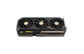
ロセッサー1を選択
ロセッサー2を選択
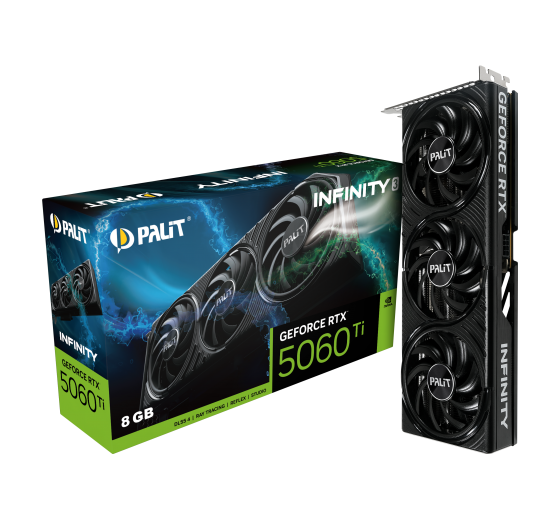
NVIDIA GeForce GTX 1070
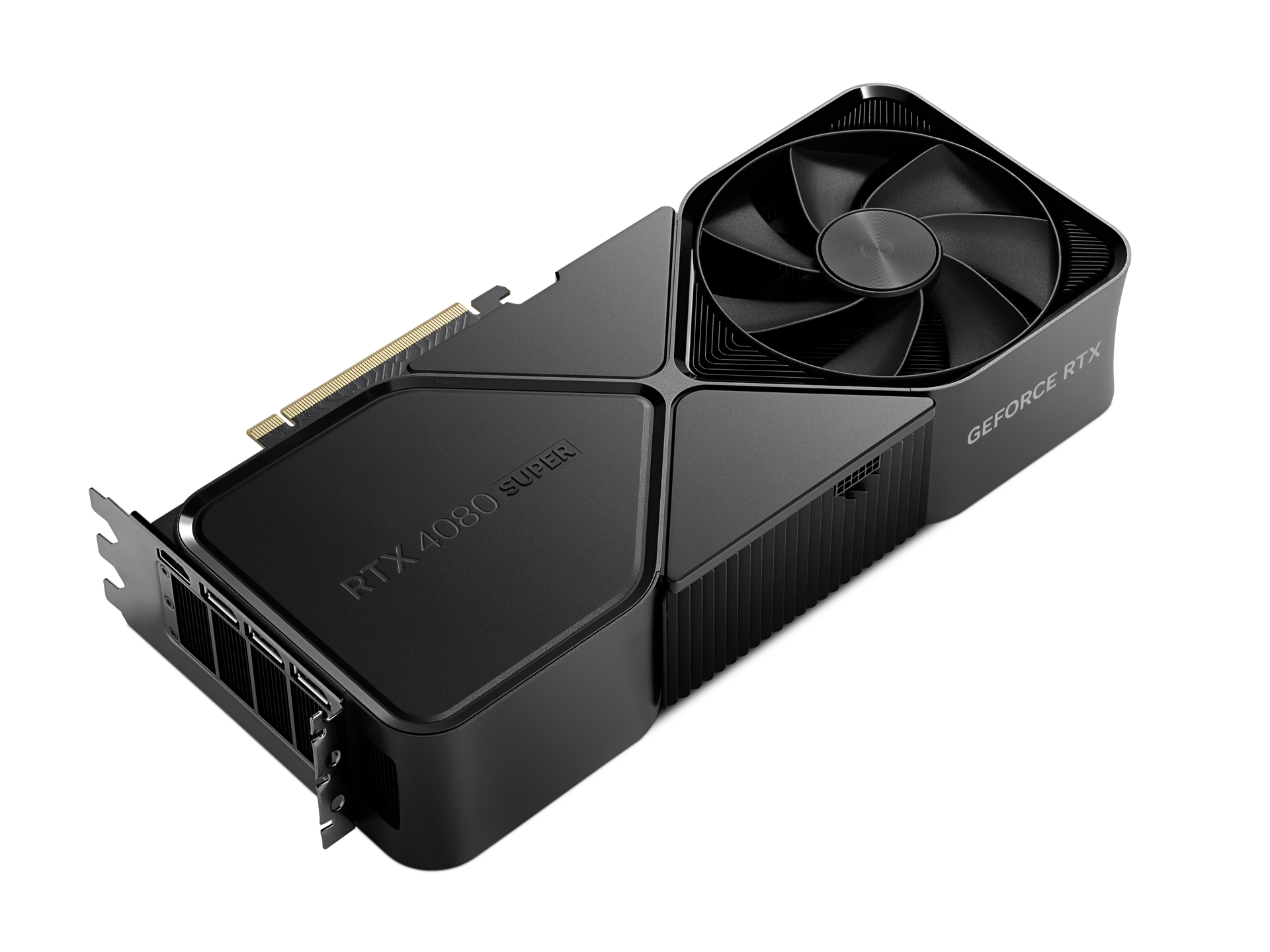
NVIDIA H100 PCIe

NVIDIA GeForce GTX 1070 対 NVIDIA H100 PCIe. 仕様・性能・テスト

User rating
star star star star star
発売済み
Q3/2016
NVIDIA GeForce GTX 1070
発売済み
Q2/2022
User rating
star star star star star
NVIDIA H100 PCIe
NVIDIA H100 PCIe

ベストな選択とは NVIDIA GeForce GTX 1070 または NVIDIA H100 PCIe? どのグラフィックカードが速い?

Compare the available specifications of these models.

NVIDIA GeForce GTX 1070 has a base frequency of 2 GHz. メモリサイズ 8 GB. メモリータイプ GDDR5. で発売されました。 Q3/2016.

NVIDIA H100 PCIe has a base frequency of 1.065 GHz. メモリサイズ 80 GB. メモリータイプ HBM2e. で発売されました。 Q2/2022.

相違点

  • クロックの高速化

    周辺 88% クロックスピードの向上

    2 GHz left arrow 1.065 GHz
  • その他のメモリ

    900メモリ増量

    80 GB left arrow 8 GB

仕様

技術データ
NVIDIA GeForce GTX 1070 NVIDIA GeForce GTX 1070
NVIDIA H100 PCIe NVIDIA H100 PCIe
一般情報

グラフィックスカードの基本技術データの比較 NVIDIA GeForce GTX 1070 と NVIDIA H100 PCIe, チップ、情報処理装置.

  • 建築
    Pascal left arrow Hopper
  • Execution Units
    1920 left arrow 7296
  • GPUチップ
    GP104 left arrow GH100
  • L1 Cache
    48 KB left arrow -
  • L2 Cache
    2 MB left arrow -
  • レンダリング出力単位
    64 left arrow 24
  • テクスチャユニット
    120 left arrow 456
メモリ設定

Video memory capacity, type, bus width and bandwidth describe different properties. These values alone do not determine graphics performance.

  • Memory Bandwidth
    256.3 GB/s left arrow 1,280 GB/s
  • Memory Bus
    256 bit left arrow 5120 bit
  • Memory Clock
    2000 MHz left arrow 1000 MHz
  • Memory Data Rate
    8 Gbps left arrow 2 Gbps
  • メモリサイズ
    8 GB left arrow 80 GB
  • メモリータイプ
    GDDR5 left arrow HBM2e
クロック周波数

Published GPU clock frequencies describe different operating modes. Clock speed alone does not determine graphics performance.

  • 基本周波数
    1506 MHz left arrow 1065 MHz
  • 最大周波数
    1683 MHz left arrow 1650 MHz
エネルギー消費量

Graphics card power limits and recommended system power supply describe different specifications.

  • System Power Supply
    450 W (PSU recommendation) left arrow 750 W (PSU recommendation)
  • TDP
    150 W left arrow 350 W
インターフェイス

コネクティビティと接続.

  • DisplayPort Ports
    3 × DisplayPort 1.4a left arrow -
  • DVIポート
    1 × DVI left arrow -
  • HDMI端子
    1 × HDMI 2.0 left arrow -
  • Max. 表示数
    5 left arrow 1
  • PCIe Interface
    PCIe 3.0 x16 left arrow PCIe 5.0 x16
  • Power Connectors
    1x 8-pin left arrow 8-pin EPS
技術データ

コンピュータゲームに活かされる技術データ.

  • CUDA
    6.1 left arrow 9.0
  • DirectX
    12.1 left arrow いいえ
  • 最大解像度
    3840 × 2160 left arrow -
  • OpenCL
    3.0 left arrow 3.0
  • OpenGL
    4.6 left arrow いいえ
  • Shader Model
    6.7 (6.4) left arrow いいえ
  • Vulkan
    1.3 left arrow いいえ
外形寸法図

比較したデバイスのサイズ、重量、スロットの違い

  • 高さ
    40 mm left arrow -
  • 長さ
    267 mm left arrow -
  • Slot Size
    Dual-slot left arrow -
  • Width
    112 mm left arrow -
詳細はこちら

GPUのインターフェースと発売時期の比較 NVIDIA H100 PCIe と NVIDIA GeForce GTX 1070.

  • Process Technology
    16 nm left arrow 4 nm
  • 発売日
    Q3/2016 left arrow Q2/2022
Theoretical Performance

  • FP16 (theoretical)
    101.0 GFLOPS (1:64) left arrow 96.31 TFLOPS
  • FP32 (theoretical)
    6.463 TFLOPS left arrow 24.08 TFLOPS
  • FP64 (theoretical)
    202.0 GFLOPS (1:32) left arrow 12.04 TFLOPS
  • Pixel Rate
    107.7 GPixel/s left arrow 39.60 GPixel/s
  • Texture Rate
    202.0 GTexel/s left arrow 752.4 GTexel/s

ベンチマーク

性能試験 GPUs
Individual model tests

These results have no shared test of both models with the same version and settings. They are shown separately without a percentage difference.

NVIDIA GeForce GTX 1070

More results: 9

NVIDIA H100 PCIe

最新の比較