ベストな選択とは AMD Radeon RX 570 または NVIDIA RTX A4500? どのグラフィックカードが速い?
最適なグラフィックカードを選ぶために、比較を用意しました。それぞれの仕様やベンチマークを比較してみてください。
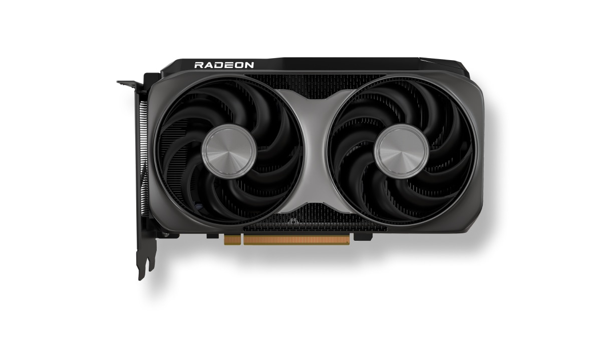
AMD Radeon RX 570 has a base frequency of 1.75 GHz. メモリサイズ 4 GB. メモリータイプ GDDR5. で発売されました。 Q2/2017.
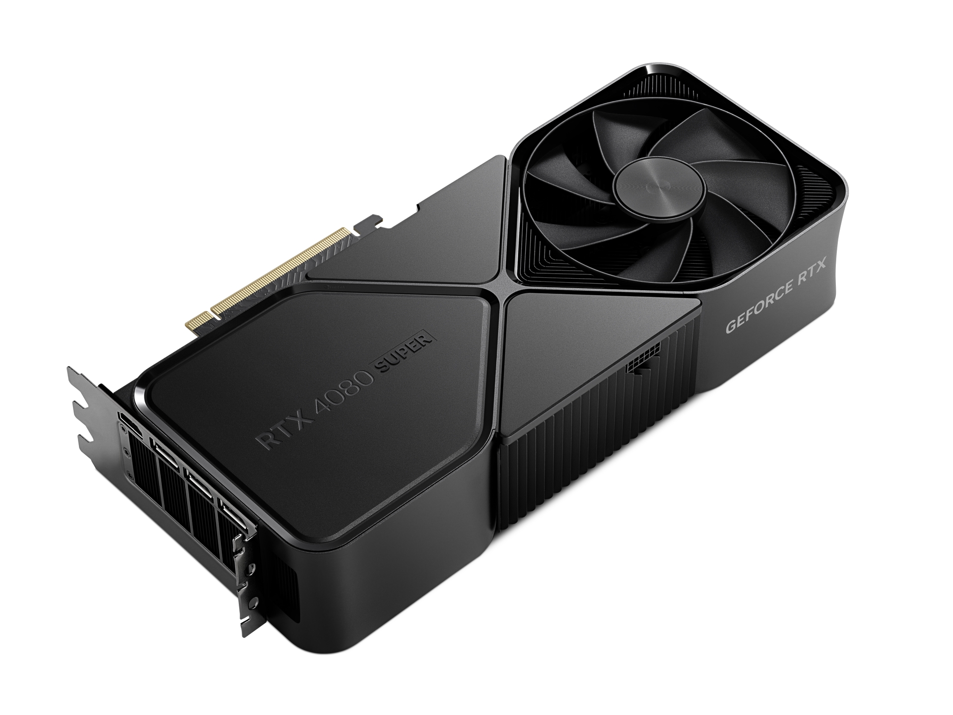
NVIDIA RTX A4500 has a base frequency of 2 GHz. メモリサイズ 20 GB. メモリータイプ GDDR6. で発売されました。 Q4/2021.
考慮すべき理由 共通ポジション AMD Radeon RX 570 他機種との比較のため、一般的なベンチマークでGPUを使用。.
考慮すべき理由 クロックの高速化
周辺 14% クロックスピードの向上
 1.75 GHz
その他のメモリ
400メモリ増量
4 GB
共通ポジション NVIDIA RTX A4500 他機種との比較のため、一般的なベンチマークでGPUを使用。.
AMD Radeon RX 570
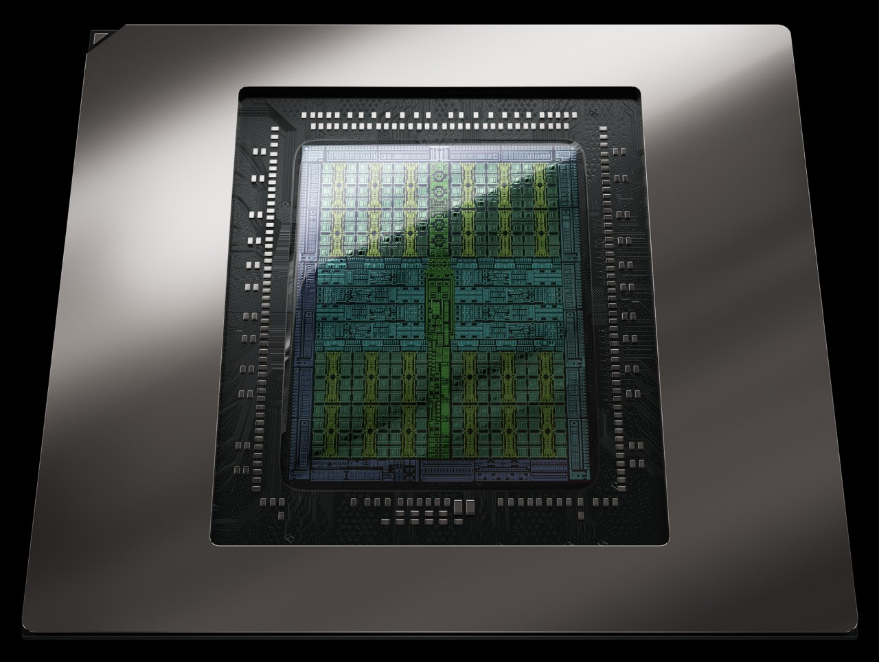
グラフィックスカードの基本技術データの比較 AMD Radeon RX 570 と NVIDIA RTX A4500, チップ、情報処理装置.
 Ampere
56
GA102
96
7168
224
Ampere
56
GA102
96
7168
224
Video memory capacity, type, bus width and bandwidth describe different properties. These values alone do not determine graphics performance.
20 GB
2000 MHz
GDDR6
Published GPU clock frequencies describe different operating modes. Clock speed alone does not determine graphics performance.
1050 MHz
1650 MHz
Graphics card power limits and recommended system power supply describe different specifications.
200 W
コネクティビティと接続.
4
PCIe 4.0 x16
コンピュータゲームに活かされる技術データ.
12.2
はい
7680 × 4320
はい
動画・画像圧縮規格に対応した内蔵型.
Decode
Decode / Encode
Decode / Encode
Decode
Decode
GPUのインターフェースと発売時期の比較 NVIDIA RTX A4500 と AMD Radeon RX 570.
NVIDIA
8 nm
Q4/2021
These results have no shared test of both models with the same version and settings. They are shown separately without a percentage difference.
いくつかの一般的なベンチマークの結果に基づき、より正確に、次のような性能差を見積もることができます AMD Radeon RX 570 と NVIDIA RTX A4500.
合成ベンチマークを比較して、あなたに最適なグラフィックカードを選びましょう
These are saved results from the earlier catalog. Measurement dates and test configurations were not recorded. Models with no comparable results are omitted.
Recent models: test results with identified primary sources — Game frame rates
Archived results. The original measurement method and test conditions have not been verified.
Higher values are better in this metric.


 English
 Russian
 German
 Portuguese
 Italian
 French
 Spanish
 Polish
 Chinese
 Korean